TLP250 Mosfet Driver (#157)
ج.م60.00
Learn More
Pin configuation isolated mosfet driver TLP250
Pin layout of TLP250 is given below. It is clearly shown in figure that led at input stage and photo detector diode at output stage is used to provide isolation between input and ouput. Pin number 1 and 4 are not connected to any point. Hence they are not in use. Pin 2 is anode point of input stage light emitting diode and pin 3 is cathode point of input stage. Input is provided to pin number 2 and 3. Pin number 8 is for supply connection. Pin number 5 is for ground of power supply.
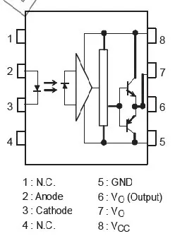
- Pin number one and four is not connected to any point physically. Therefore they are not in use.
- Pin number 8 is use to provide power supply to TLP250 and pin number 5 is ground pin which provides return path to power supply ground. Maximum power supply voltage between 15-30 volt dc can be given to TLP250. But it also depends on temperature of environment in which you are using TLP250.
- Pin number 2 and 3 are anode and cathode points of input stage LED. It works like a normal light emitting diode. It has similar characteristics of forward voltage and input current. Maximum input current is in the range of 7-10mA and forward voltage drop is about 0.8 volt. TLP250 provides output from low to high with minimum threshold current of 1.2mA and above.
- Pin number six and seven is internally connected to each other. Ouput can be taken from either pin number 6 and 7. Totem pole configuration of two transistor is used in TLP250. In case of high input , output becomes high with output voltage equal to supply voltage and in case of low input, output become low with output voltage level equal to ground.
- Mosfet driver TLP250 can be used up to 25khz frequency due to slow propagation delay.